Spin Qubits in Semiconductor Quantum Dots
Imagine shrinking a piece of semiconductor material until its dimensions reach just a few nanometers. At this incredibly small scale, the laws of classical physics that govern our everyday experiences are no longer sufficient to describe the behavior of matter, and quantum mechanics becomes essential. One of the most fascinating structures that emerges at this scale is the quantum dot—an extremely small island capable of confining electrons within a tightly restricted three-dimensional region.
To better understand this confinement, we must first introduce the concept of the Fermi wavelength () This wavelength provides a characteristic length scale at which the wave-like nature of electrons becomes significant. When the dimensions of a structure become comparable to or smaller than this length scale, quantum confinement becomes increasingly important. If the dimensions are sufficiently small in all three spatial directions, electrons can no longer move freely, resulting in a zero-dimensional system [4, 2].
Once an electron is confined within such a small region, its behavior and energy can be described using the time-independent Schrödinger equation. By solving this equation for a particle confined within a three-dimensional box, we obtain an expression for its quantized energy levels, given by:
In this expression,denotes the reduced Planck constant,represents the effective mass of the electron, the parameters,, anddescribe the physical dimensions of the box along the three spatial directions, and the variables,, andare positive integers known as quantum numbers [2].
Since the dimensions of the quantum dot, represented by theparameters, appear in the denominators of the fractions, reducing the size of the confined region increases the energy associated with each quantum state and enlarges the spacing between the allowed energy levels. In other words, the electron's energy in this confined space no longer forms a continuous spectrum in which any energy value is possible; instead, it becomes discrete, or quantized. This quantization is so pronounced that the density of states (DOS), which typically forms a continuous distribution in bulk materials, collapses into a series of sharp, well-separated peaks in quantum dots [2].
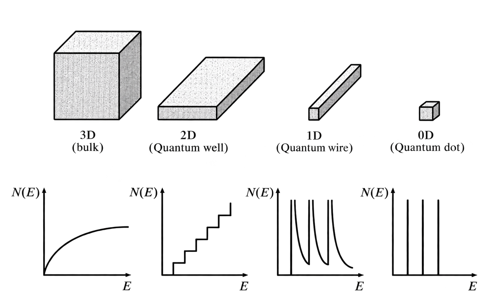
Figure 1. Comparison of three-dimensional, two-dimensional, one-dimensional, and zero-dimensional structures (quantum dots), along with their corresponding densities of states [2].
Such strong spatial confinement allows a quantum dot to exhibit behavior resembling that of an individual atom, even though it may consist of thousands of atoms. For this reason, scientists refer to these structures as artificial atoms. Unlike naturally occurring atoms, however, these man-made structures offer the flexibility to tailor their properties and energy levels by adjusting their physical dimensions [4, 2].
The ability to precisely tune energy levels and control individual electric charges has made gate-defined quantum dots one of the most promising platforms for quantum information processing [4, 1].
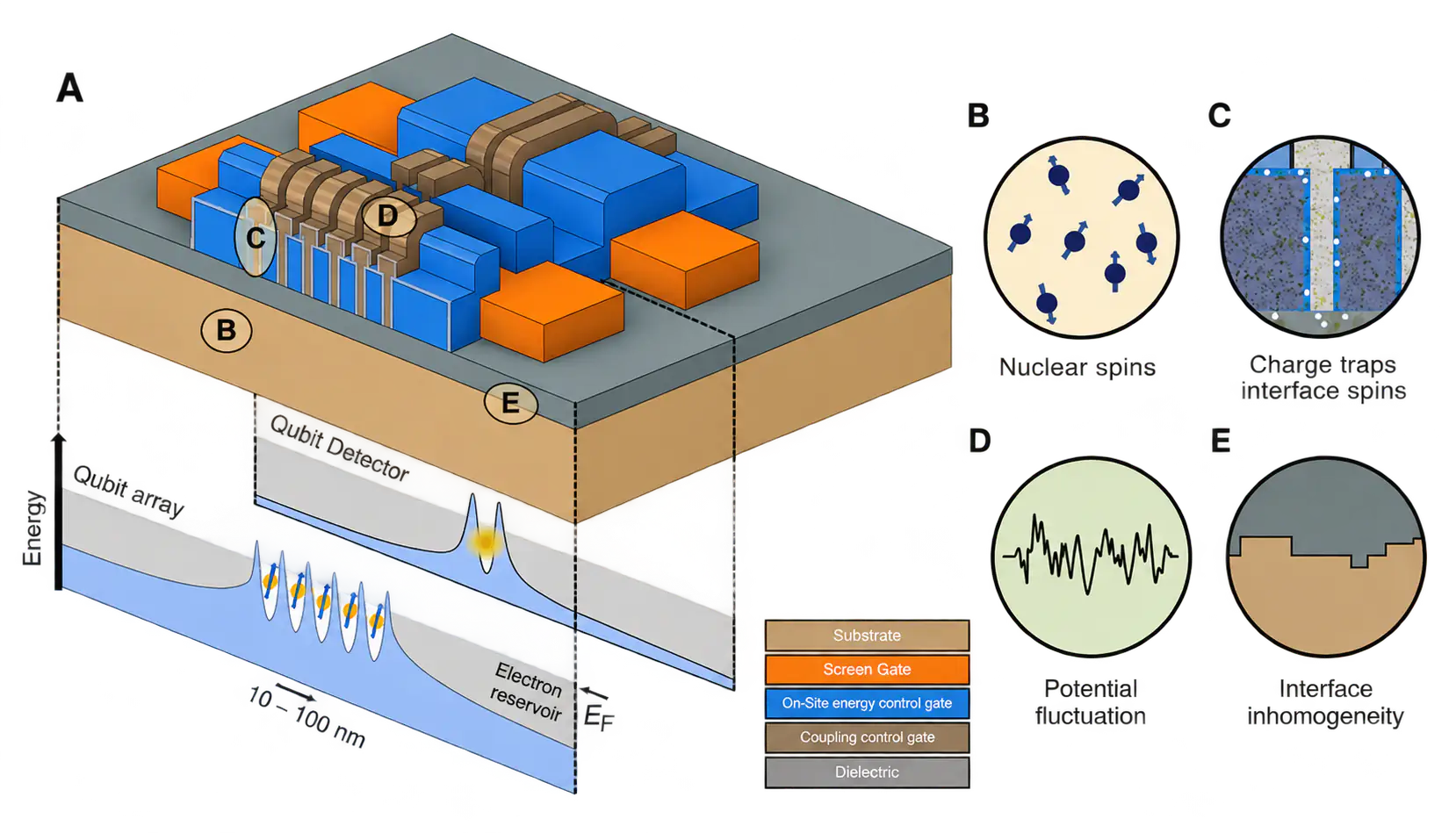
Figure 2. Semiconductor Quantum-Dot Spin Qubits (A) Schematic illustration of a gate-defined semiconductor quantum-dot spin-qubit device. These qubits exploit the spin states of individual electrostatically confined electrons or holes, together with exchange coupling between spins, to perform single-qubit and two-qubit operations. The main gate layers consist of screening gates (orange), local energy-control gates (blue), and interdot tunnel-coupling control gates (brown), which are electrically isolated from one another by thin dielectric layers (gray). (B) Nuclear-spin fluctuations in the substrate, which can be a major source of noise for spin qubits. (C) Charge traps and two-level fluctuators that may be present at the dielectric interface. (D) Environmental electrical noise affecting the tuning of quantum-dot energy levels and tunnel coupling. (E) Imperfections at the interface between the substrate and the upper layer, resulting in potential inhomogeneities and valley splitting [1].
In this architecture, rather than relying on physical walls, a carefully engineered network of nanoscale metal electrodes is used to create an electrostatic potential profile that locally confines charge carriers. At the bottom of the structure lies the semiconductor substrate, which forms the foundation of the device [1]. Within this substrate, electron motion is strongly restricted along one spatial direction, allowing the particles to move relatively freely within an extremely thin, two-dimensional plane. This system is known as a two-dimensional electron gas [2].
A key property of this electron gas is its high mobility, a measure of how readily charge carriers move through a material under an applied electric field. High mobility indicates that electrons can travel with relatively little scattering from impurities and other defects [1]. To prevent electrical current from leaking between the control electrodes and the underlying semiconductor, a thin dielectric insulating layer is deposited on the substrate, electrically isolating the upper gate electrodes.
The gate architecture begins with the first electrode layer, consisting of screening gates. By applying a negative voltage to these orange-colored electrodes, a repulsive electrostatic potential is created beneath them. This potential barrier depletes the two-dimensional electron gas of free electrons in the regions directly underneath the gates, leaving a narrow, well-defined channel through which the remaining electrons can move.
The next step is to divide this channel into separate quantum dots using blue-colored electrodes known as local energy-control gates. By appropriately adjusting the voltages applied to these gates, the local potential landscape can be modified to create potential wells within the channel, attracting electrons into nanoscale regions where they become confined [1].
Electron confinement in these wells is accompanied by Coulomb blockade, a phenomenon in which the electrostatic repulsion between electrons makes it energetically costly to introduce an additional electron into a quantum dot. The energy required to add one more electron is approximately given bywhereis the elementary charge andis the capacitance of the quantum dot [2]. Because quantum dots are extremely small, their capacitance is very low. Since capacitance appears in the denominator of this expression, a reduction in capacitance significantly increases the energy required to add another electron [4, 2].
This mechanism enables researchers to control and determine the number of electrons confined within each quantum dot one by one—a fundamental prerequisite for initializing and manipulating qubits in quantum processors [1].
The next stage involves precisely manipulating these particles to perform logical operations. In this architecture, quantum information is encoded in the spin degrees of freedom of electrons. To change the state of an individual qubit, resonant microwave pulses are applied [1]. When the frequency of these electromagnetic pulses matches the energy splitting between the two spin states, the electron spin can be driven into controlled rotation, allowing it to be placed in an arbitrary superposition of its two basis states. This process forms the foundation of single-qubit gates [1].
However, the true computational power of a quantum computer lies in establishing quantum correlations and entanglement between neighboring qubits. This task is performed by the brown-colored electrodes known as coupling-control gates [1]. Positioned between the blue local energy-control gates, these electrodes regulate the height of the electrostatic potential barrier separating adjacent quantum dots [1].
By adjusting the voltages applied to the brown gates and temporarily lowering this barrier, the wave functions of electrons in neighboring quantum dots can penetrate the intervening region and overlap with one another [1]. This physical overlap gives rise to the Heisenberg exchange interaction, which can be described by the quantum Hamiltonian. Here,andare the spin operators of the two electrons, whileis the parameter that determines the strength of their exchange interaction [4]. The exchange couplingis not necessarily constant; its magnitude can be controlled by adjusting the voltages applied to the gate electrodes, which in turn modify the interdot tunneling rate.
During this interaction, the spin states of the two electrons become coupled, enabling the implementation of a two-qubit gate and the generation of entanglement [1]. Combining microwave-driven single-spin rotations with exchange interactions arising from interdot coupling is sufficient to realize a universal set of quantum gates, making it possible to implement complex quantum algorithms on this hardware platform [4, 5].
Following computation, the final stage is the readout of quantum information. Directly measuring the spin state of a single electron is extremely challenging because of its weak magnetic moment. To overcome this limitation, these devices employ a technique known as spin-to-charge conversion.
In the lower part of Figure 2, a structure called a qubit detector can be seen adjacent to the qubit array. This detector is essentially a single-electron transistor that functions as an ultrasensitive electrometer, capable of detecting even the movement of a single electron in its surrounding environment through the resulting change in electrical signal.
Adjacent to this sensing system is an electron reservoir, whose electron population is characterized by a parameter known as the Fermi energy, [1]. The Fermi energy represents the highest occupied electron energy level at absolute zero and serves as an energy reference for electron exchange in this architecture [2].
To extract information from the qubit, energy-selective tunneling or Pauli spin blockade can be employed [1]. Pauli spin blockade arises directly from the Pauli exclusion principle, which states that no two identical fermions, such as electrons, can occupy the same quantum state simultaneously [4, 2].
By appropriately tuning the voltages applied to the control gates, the system can be configured so that an electron can tunnel into a neighboring quantum dot only when the resulting two-electron configuration is compatible with the spin and orbital selection rules. In the standard Pauli spin-blockade readout scheme, two electrons with opposite spins can form a singlet state, characterized by an antisymmetric spin wave function. In contrast, a triplet state belongs to one of three symmetric spin configurations: one with parallel spins and two with antiparallel spins in symmetric superpositions.
Because of the symmetry requirements imposed by the Pauli exclusion principle, a triplet state may be prevented from transitioning into a doubly occupied ground state of the neighboring dot when that state is accessible only to a singlet configuration. Consequently, electron tunneling is blocked [4].
Whether or not the electron transfers to the neighboring dot is then detected by the nearby electrometer through the resulting change in the local charge distribution. In this way, the spin state is converted into a classical electrical signal that can be measured electronically, allowing the final qubit state to be determined with high accuracy without requiring complex magnetic sensors [1].
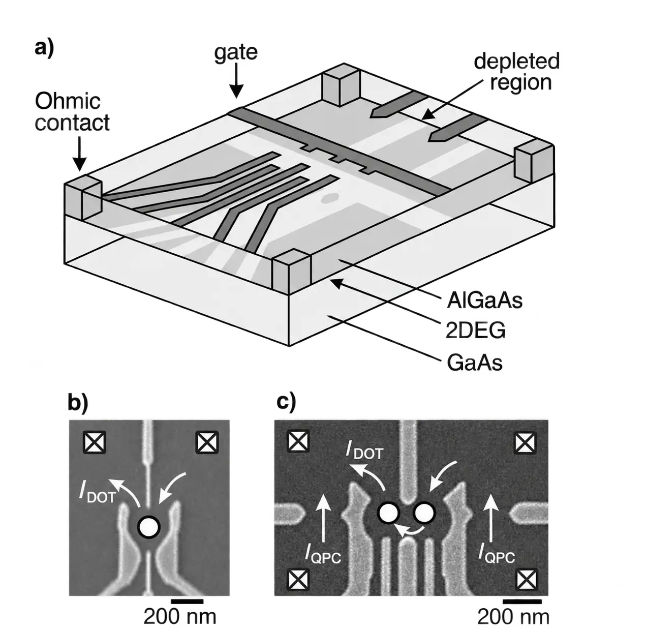
Figure 3. Lateral Quantum-Dot Device Defined by Surface Metal Gates(a) Schematic illustration of a lateral quantum-dot device. Negative voltages applied to the gates (dark gray) create depleted regions (white) within the electron gas. (b) and (c) Scanning electron microscopy (SEM) images of a single multielectron quantum dot and a double quantum dot, respectively. The white circles indicate the locations of the quantum dots. In device (c), the adjacent gates serve as a charge sensor (electrometer) [4].
Despite the ability to coherently control these quantum states, the unavoidable interaction between a quantum system and its surrounding environment gives rise to quantum noise and decoherence [1].
During the early stages of this technology's development, researchers fabricated quantum dots in semiconductor heterostructures such as gallium arsenide (GaAs). However, they soon encountered a fundamental physical limitation. The constituent nuclei of these materials, including the isotopes gallium-69, gallium-71, and arsenic-75, possess nuclear spin. Through the hyperfine interaction, a magnetic interaction between the electron spin and the magnetic fields generated by atomic nuclei, these nuclear spins couple to the qubit [4, 1].
The presence of this vast ensemble of nuclei produces a fluctuating, random magnetic field within the material. When the electron spin is exposed to these fluctuations, the qubit's quantum state rapidly loses coherence. A major challenge with materials such as GaAs is that all their stable isotopes have nonzero nuclear spin. Consequently, eliminating nuclear spins and their associated magnetic fields from the GaAs crystal lattice is not a viable option [1].
This fundamental limitation became a major motivation for researchers to turn to silicon (Si). In naturally occurring silicon, the abundance of isotopes with nonzero nuclear spin is relatively low: only approximately 4.7% consists of silicon-29, which has a nuclear spin ofNevertheless, to suppress magnetic noise further and extend coherence times, advanced isotopic purification techniques are employed to remove even this small fraction of nuclear-spin-bearing isotopes from the semiconductor material.
In this approach, processes such as chemical vapor deposition (CVD) are used to grow thin, single-crystalline layers of silicon enriched in silicon-28 on suitable substrates. Silicon-28 has zero nuclear spin. Using isotopically enriched silicon suppresses hyperfine-field fluctuations and has led to substantial improvements in coherence times, in some cases by more than an order of magnitude. The success of this strategy has also encouraged efforts to purify other materials, including germanium (Ge), by reducing the abundance of germanium-73, which has a nuclear spin of. These efforts aim to establish increasingly robust platforms for future quantum computers [1].
Because gate-defined quantum dots rely on the precise tuning of electrostatic potentials, any unwanted fluctuation in the surrounding charge distribution can alter these local potentials. The origins of such parasitic charges are often associated with different stages of device fabrication. During high-energy processes, including plasma-based treatments and ion implantation, stray charges may penetrate the dielectric layers or become trapped at interfaces between the dielectric and the semiconductor.
These trapped charges, together with structural defects in dielectric layers and at material interfaces, can form microscopic structures known as two-level systems. Such systems can be modeled as having a double-well potential, allowing a trapped atom or charge to switch randomly between two metastable configurations [1].
These random transitions generate slow fluctuations in the background charge environment, producing what is known asnoise. In this type of noise, the noise power increases as the frequency decreases. Consequently, slower fluctuations can have a particularly detrimental effect on the stability of the system. Measurements indicate that the characteristic amplitude of these fluctuations is typically on the order of a few microelectronvolts. Despite their small magnitude, these fluctuations can limit the ultimate precision, or fidelity, of both single-qubit and two-qubit gates.
In addition to stray charges, mechanical stresses at metal–semiconductor interfaces present another significant challenge. These stresses generate strain fields, which distort the crystal lattice. Ideally, the device should provide a smooth electrostatic pathway with well-defined, controllable potential wells. However, strain-induced distortions can introduce unwanted bends and irregularities into the electrostatic landscape, creating unintended potential wells along the channel.
These parasitic quantum dots can trap passing electrons, preventing them from reaching their intended destinations. This phenomenon not only reduces the number of useful charge carriers and depletes carriers in neighboring regions, but also turns each trapped electron into an additional source of charge noise, generating further electrical fluctuations in the surrounding environment [1].
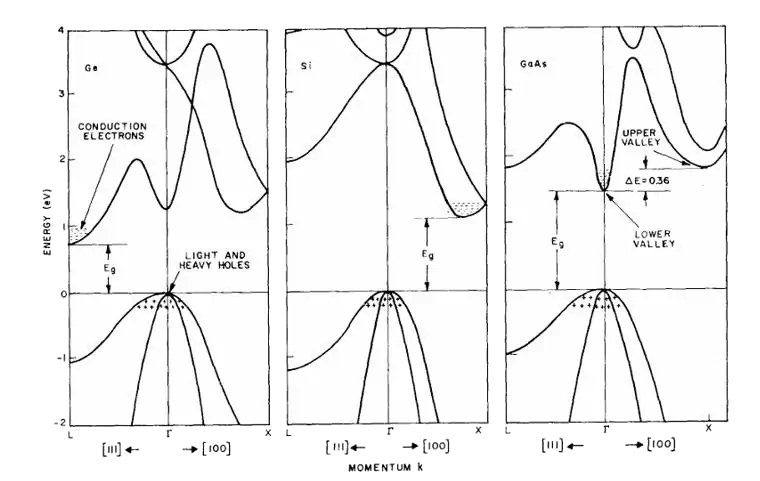
Figure 4. Energy band structures as a function of crystal momentum for germanium (Ge), silicon (Si), and gallium arsenide (GaAs) [3].
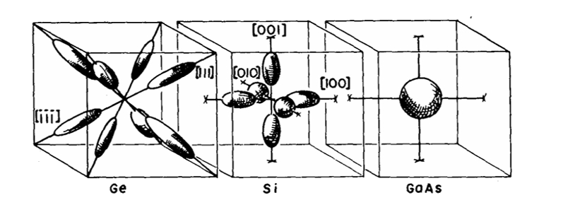
Figure 5. Constant-energy surfaces in the Brillouin zone for germanium (Ge), silicon (Si), and gallium arsenide (GaAs). In Ge, eight ellipsoidal valleys are oriented along thedirections, with the Brillouin-zone boundaries passing through the centers of these ellipsoids. In Si, six ellipsoidal valleys are oriented along thedirections, with their centers located approximately three-quarters of the way from the Brillouin-zone center toward its boundary. In GaAs, the constant-energy surface is spherical and centered at the zone center [3].
One of the other major sources of disorder in silicon quantum dots lies at the interface between silicon and its surrounding dielectric layer [1].
In a semiconductor with a direct band gap, such as gallium arsenide, the conduction-band minimum lies precisely at the center of the first Brillouin zone, at the point denoted by, where the crystal momentum is zero:.
In this structure, the conduction-band minimum is located at a single point in momentum space, meaning that electrons occupy a single valley at the band edge. In silicon, however, which is an indirect-band-gap semiconductor, the situation is different. The conduction-band minimum does not lie at the center of the Brillouin zone but instead occurs along thecrystallographic directions. Owing to the symmetry of silicon's cubic crystal lattice, six distinct, equivalent, ellipsoidal energy valleys emerge in momentum space. The degeneracy of these six valleys gives rise to valley degeneracy in the system [3].
To create a spin qubit, electrons are confined within a thin, two-dimensional layer at the silicon interface. This strong spatial confinement breaks part of the system's symmetry, lifting the energy degeneracy of some of the valleys. As a result, four valleys shift to higher energies because of their orientation relative to the confinement direction, while the remaining two valleys retain equal energies and remain degenerate.
In quantum computing, the persistence of these two equivalent valleys presents a challenge because reliable information processing requires a well-defined and sufficiently isolated quantum ground state. Consequently, the residual degeneracy must be lifted through precise strain engineering and the careful tuning of electric fields at the material interface. This process, known as valley splitting, separates the corresponding energy levels and is crucial for achieving long coherence times and reliable qubit readout.
Nevertheless, no interface is perfectly smooth or defect-free at the nanometer scale. Atomic-scale steps and structural defects introduce spatial variations in the magnitude of valley splitting across the processor [1].
Despite significant progress in the development of silicon quantum dots, researchers continue to explore alternative material platforms to overcome existing limitations and improve stability at scale. One particularly promising direction is the use of hole-spin qubits in the valence bands of materials such as germanium and silicon [1].
The strength of the contact hyperfine interaction between a particle and nuclear spins depends directly on the probability density of the particle's wave function at the nucleus, expressed as.Conduction-band electrons often have substantial \(s\)-orbital character, whose wave functions are nonzero at the nucleus. Thus,.This makes them particularly susceptible to magnetic noise arising from nuclear spins.
By contrast, valence-band holes have predominantly-orbital character. Because a-orbital wave function has a node at the nucleus, its value at the nuclear position vanishes:.
As a result, the contact hyperfine interaction is significantly suppressed for valence-band holes, potentially enabling substantially longer coherence times [4, 1].
In addition to their reduced sensitivity to nuclear magnetic noise, holes exhibit intrinsically strong spin–orbit coupling. This property enables rapid electrical control of their quantum spin states without requiring additional components to generate local magnetic fields. Consequently, auxiliary devices such as micromagnets may not be necessary for qubit manipulation [1].
Beyond conventional semiconductors, carbon-based structures have also emerged as promising hosts for spin qubits. Carbon nanotubes and multilayer graphene offer considerable potential for realizing quantum dots with long coherence times. In particular, their nuclear-spin-related magnetic noise can be reduced through isotopic purification using carbon-12, which has zero nuclear spin.
Recent advances in controlling structural disorder in graphene have further raised the possibility of exploiting both spin and valley degrees of freedom simultaneously for quantum information storage and processing in future devices [1].
Moving beyond individual qubits toward scalable, fault-tolerant quantum processors requires fundamental advances in how materials are discovered and characterized. Precisely identifying the microscopic origins of noise under demanding conditions—including ultrahigh vacuum, millikelvin temperatures, and subnanometer length scales—remains extremely challenging. This calls for high-throughput approaches that combine quantum measurements with direct materials spectroscopy.
Ultimately, overcoming these structural and materials-related challenges will require more than advances in physics alone. It will depend on close interdisciplinary collaboration among materials scientists, chemists, and quantum engineers [1].
References
[1] De Leon, N. P., Itoh, K. M., Kim, D., Mehta, K. K., Northup, T. E., Paik, H., ... & Steuerman, D. W. (2021). Materials challenges and opportunities for quantum computing hardware. Science, 372(6539), eabb2823.
[2] G. W. Hanson, Fundamentals of Nanoelectronics, Pearson Education
[3] S. M. Sze, Physics of Semiconductor Devices, Wiley
Hanson, R., Kouwenhoven, L. P., Petta, J. R., Tarucha, S., & Vandersypen, L. M. (2007). Spins in few-electron quantum dots. Reviews of modern physics, 79(4), 1217-1265. [4]
[5] M. A. Nielsen and I. L. Chuang, Quantum Computation and Quantum Information, Cambridge University Press