The key advantage of quantum information processing lies in its ability to outperform even the world’s most powerful classical supercomputers. This technology has the potential to solve highly complex problems, including the simulation of quantum systems, factoring algorithms, search problems, and optimization tasks—computations that lie beyond the practical capabilities of today’s computers. This advantage arises from a fundamental difference in how information is encoded and processed in quantum systems compared with their classical counterparts.
Information processing in classical computers is based on units called bits, each of which can exist in only one of two definite states, 0 or 1. In this architecture, a classical N-bit register encodes information using N binary coefficients. In contrast, a qubit, the fundamental unit of quantum information processing, can exist in a linear combination of the basis statesand.
When the system is extended to a register consisting of N qubits, it can simultaneously exist in a superposition of allpossible combinations of these basis states. A complete description of such a system requirescontinuous complex-valued coefficients, resulting in an exponential increase in the information-storage capacity[1].
To formulate this complex behavior mathematically, quantum mechanics employs the concept of Hilbert space, a complex vector space in which the state of any isolated physical system is represented by a unit vector. The dimensionality of this space grows so rapidly with the number of qubits that describing a system of only 500 qubits requires a space whose number of dimensions exceeds the estimated number of atoms in the universe.
Although visualizing the Hilbert space of multi-qubit systems is practically impossible, a geometric model known as the Bloch sphere is commonly used to provide an intuitive representation of a single qubit. On this unit sphere, the north and south poles represent the classical states 0 and 1, respectively, while a quantum superposition state can lie at any point on the surface of the sphere, representing a continuous range of possible states[2].
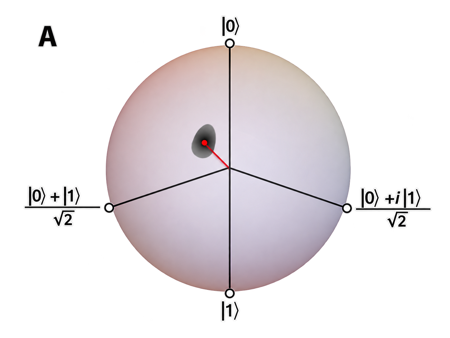
Figure 1. Representation of a single-qubit state on the Bloch sphere. The shaded region represents the deviation of the state vector from the ideal state (error) caused by factors such as decoherence or imperfections in quantum gate operations [1].
Entanglement, whose significance has been compared to that of the discovery of iron in the Bronze Age of the classical world, links qubits so strongly that the state of one cannot be described independently of the other[2]. By exploiting this entanglement, quantum algorithms make use of interference, analogous to the interference of physical waves. With careful design, an algorithm can be engineered so that computational paths leading to the correct answer are reinforced through constructive interference, while undesirable outcomes cancel one another through destructive interference.
However, this enormous computational potential comes at the cost of system fragility. During computation, quantum states are highly susceptible to decay and decoherence, leading to the rapid accumulation of errors in large-scale systems[1]. In classical systems, information is protected against noise by incorporating redundant data¹ and continuously monitoring the output to apply appropriate decoding and error-correction procedures. In quantum mechanics, however, any measurement or observation destroys the superposition state and collapses the system into definite values. Classical error-correction methods are therefore inadequate in this context and would make information recovery impossible[1,2].
For this reason, the development of systems capable of executing complex algorithms and implementing quantum error correction is not merely a challenge in physics; it also requires major advances in materials science and novel fabrication techniques to protect qubits against environmental noise. To date, much of the research effort in hardware development has focused on designing sophisticated architectures and control schemes to circumvent sources of noise, energy loss, and decoherence, rather than directly confronting the underlying physical limitations of materials.
This conservative strategy, however, will not be sufficient for the future realization of large-scale processors capable of efficiently executing quantum error-correction algorithms. Rather than concealing or circumventing noise, it must be eliminated at its root, at the atomic and structural levels, which requires advances in materials science and engineering. Among the available platforms, superconducting qubits are regarded as one of the most mature and leading hardware approaches for quantum information processing. Nevertheless, the scalability of this technology is currently constrained by subtle and often hidden challenges within the material layers and interfaces from which these devices are constructed. In the following, we examine these physical limitations in detail and investigate the hidden obstacles associated with the development of material layers[1].
To understand how superconducting circuits operate, the best starting point is a classical electrical oscillator: the circuit. In this circuit, the continuous exchange of energy between the electric field of the capacitor () and the magnetic field of the inductor () produces sustained oscillations. However, if such a circuit is fabricated from conventional metals, the electrical resistance arising from electron scattering rapidly dissipates the system’s energy as heat and destroys any quantum state.
The key to overcoming this limitation is to exploit superconductivity at extremely low temperatures, where electrical resistance vanishes and electrons, mediated by vibrations of the crystal lattice, form paired particles known as Cooper pairs. Unlike individual electrons, these charged pairs behave collectively as a coherent quantum fluid and carry electrical current without energy dissipation[3].
When this superconducting circuit is isolated from its surroundings and cooled to near absolute zero, the system behaves like a quantum harmonic oscillator. In this quantized circuit, the energy of the system is no longer continuous. At sufficiently low temperatures,, and under low-loss conditions, where the energy-level broadening is much smaller than, the energy is restricted to discrete levels given by, whereis the oscillation frequency of the circuit.
The energy spacing between every pair of adjacent levels in this parabolic potential well is exactly the same and is equal to.
These equally spaced energy levels constitute a fundamental obstacle to information processing because constructing a qubit requires an isolated two-level system consisting of the ground stateand the first excited state[4,2]. If the energy spacings are identical, any microwave pulse applied to drive a transition betweenandwill also unintentionally excite higher energy levels such as, making precise control of the system impossible[4].
To overcome this limitation, the symmetry of the energy-level spacing must be broken by introducing anharmonicity into the circuit potential. This is achieved by replacing the conventional inductor with a nanoscale device known as a Josephson junction. The junction consists of two superconducting metal layers separated by an extremely thin insulating barrier, allowing Cooper pairs to quantum mechanically tunnel through the barrier[4,1].
This tunneling phenomenon gives rise to a sinusoidal relationship between the current and the superconducting phase difference, causing the Josephson junction to behave as a nonlinear inductor. This nonlinearity causes the higher energy levels to become more closely spaced. Consequently, the energy required for the first transition,,becomes distinct from the energy of the second transition,.
Thanks to this difference in transition energies, precisely controlled microwave pulses can be used to selectively address only theandlevels, thereby transforming the superconducting circuit into a practical and controllable qubit[4,1].
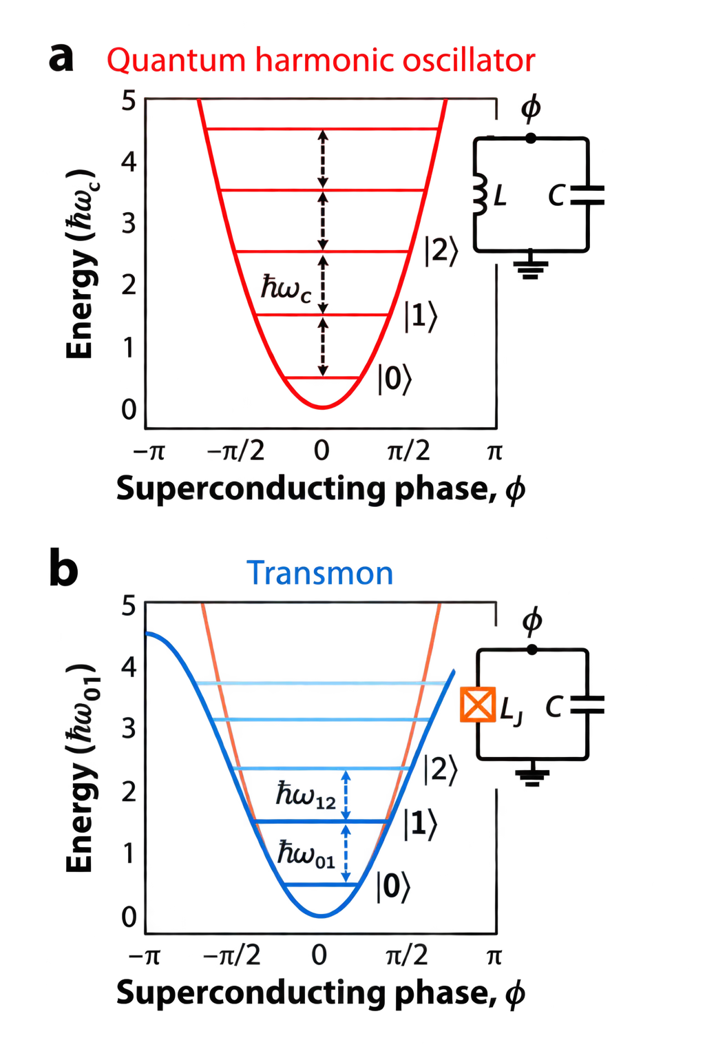
Figure 2. (a) Energy spectrum of a quantum harmonic oscillator. (b) Energy spectrum of a transmon qubit, showing the emergence of non-equally spaced energy levels due to the addition of the nonlinear Josephson junction[4].
The fabrication of Josephson junctions in superconducting qubits requires nanometer-scale precision. Because the lateral dimensions of the junction must be on the order ofto minimize energy loss, conventional optical lithography is inadequate at this scale due to the fundamental limitations imposed by optical diffraction[1]. For this reason, electron-beam lithography is employed to form a three-dimensional suspended pattern, commonly known as a shadow mask, within a resist polymer layer on the substrate surface[5,1].
Once this polymer structure has been formed, the sample is transferred into a high-vacuum chamber and the metal evaporation process begins. In the first fabrication step, aluminum is evaporated at an oblique angle relative to the substrate surface, allowing the metal atoms to pass beneath the suspended polymer bridge and form the first electrode layer on the substrate[5]. The relatively low melting point of aluminum helps ensure that the polymer mask does not melt during deposition and retains its structural integrity.
After deposition of the first layer, the tunnel barrier is formed by introducing a controlled amount of oxygen gas into the vacuum chamber[5,1]. Aluminum reacts with oxygen, but this reaction is thermodynamically self-limiting[1]. Once an aluminum oxide layer only a few nanometers thick forms on the metal surface, this newly formed oxide acts as a barrier and prevents further oxygen diffusion into the underlying layers[5,1]. This natural termination of the oxidation process makes it possible to achieve uniform control over the nanometer-scale thickness of the insulating layer without requiring complex fabrication procedures.
Another important advantage of this oxide layer is its very low density of pinholes. The presence of such microscopic defects in the insulating layer would allow electrons to flow directly through the holes rather than tunneling through the barrier, thereby creating an electrical short circuit between the two aluminum layers. This leakage current would eliminate the nonlinear behavior of the junction and disrupt the operation of the circuit[1].
After formation of the insulating barrier, the oxygen gas is evacuated and the second aluminum layer is evaporated[5,1]. In this step, the second layer is deposited at an angle different from that used for the first layer[5]. Because of this change in deposition angle, the newly deposited metal, owing to the shadow cast by the suspended polymer bridge, is positioned precisely over the oxide barrier formed on the first layer. This produces an overlap region that constitutes the final junction with the structure[5,1].
One of the key advantages of this method is that all evaporation and oxidation steps are performed in situ within a single vacuum cycle, thereby preventing environmental contaminants from reaching the junction interface[5,1]. In the final step, the remaining polymer is removed using chemical solvents in a process known as lift-off. Because aluminum is compatible with these solvents, the Josephson junction structure remains intact on the chip without sustaining damage[1].
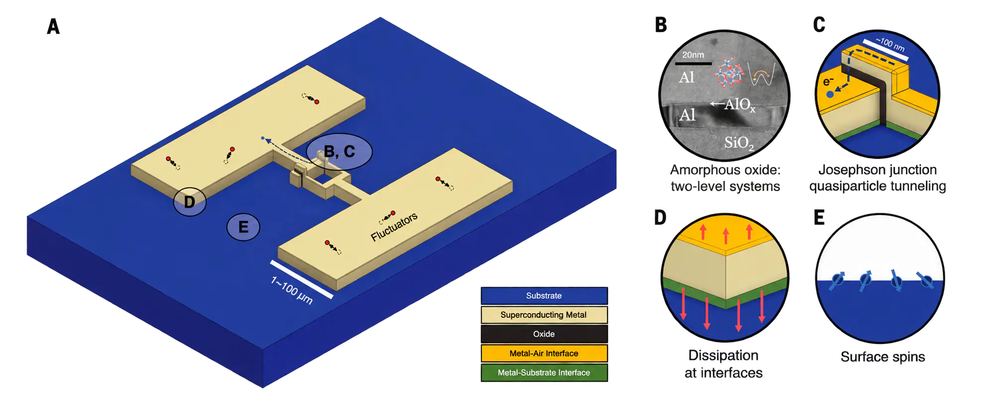
Figure 3. (A) Schematic of a superconducting transmon qubit and the primary mechanisms of noise and energy loss. (B) Cross-sectional view of the Josephson junction and two-level systems in the amorphous oxide layer. (C) Quasiparticle tunneling across the junction. (D) Dielectric loss at the device interfaces. (E) Surface spins responsible for magnetic flux noise[1].
The aluminum oxide layer,, formed during fabrication has an amorphous structure. Within this disordered structure, some atoms or bonds do not occupy fixed positions and can move between two nearby physical configurations, giving rise to what are known as two-level systems (TLSs). Each of these systems possesses an electric dipole moment that couples to the microwave electric field in the circuit. If the oscillation frequency of one of these defects matches the frequency of a qubit photon, resonance occurs, allowing the structural defect to absorb the photon and dissipate its energy through coupling to the phonon environment.
In addition to structural defects in the insulating layer, the presence of quasiparticles in the superconductor represents another source of energy loss[1]. Dissipationless current flow is achieved only when conduction electrons are bound into Cooper pairs[3]. At the operating temperatures of quantum processors, which are close to absolute zero, the population of unpaired electrons is expected to be extremely small[3,1]. Nevertheless, a small number of nonequilibrium quasiparticles are always present in the circuit as a result of excitations to energies above the superconducting gap[1], which represents the minimum energy required to break a Cooper pair into two unpaired electrons[3].
Although the precise origin of these quasiparticles remains unknown, possible mechanisms include stray visible or infrared photons, high-energy phonons, and cosmic rays. The tunneling and passage of these quasiparticles across the Josephson junction create a dissipation channel and cause decoherence of the quantum information. In the absence of a definitive identification of the origin of these excitations, materials-based strategies for mitigating quasiparticle effects include engineering the superconducting gap within the junction structure or incorporating surface traps. These traps consist of specific metallic regions with a lower superconducting gap, positioned near the qubit so that they attract and capture stray quasiparticles before the quasiparticles can reach the junction.
Alongside the Josephson junction, larger circuit components such as capacitors and inductors, which may extend to several hundred micrometers, are fabricated from materials such as aluminum, niobium, or titanium nitride. Because of the large surface area of these components, a significant fraction of the qubit’s electric field penetrates into the substrate. This field penetration gives rise to dielectric loss: impurities, charged ions, or dipoles within the substrate absorb the microwave energy stored in the qubit and dissipate it as thermal vibrations. The greater this loss, the more rapidly the qubit loses its energy and relaxes from the excited stateto the ground state. To suppress this energy leakage and extend the qubit lifetime, quantum processors are fabricated on ultra-high-purity substrates such as high-resistivity silicon or single-crystal sapphire,. Because materials such as sapphire are single crystalline, their crystal structure is free from many of the defects and imperfections associated with surfaces and interfaces, resulting in extremely low dielectric loss and allowing the qubit’s electric field to be maintained without being converted into heat.
Nevertheless, the microscopic environment surrounding the chip inevitably contains stray electric charges that continuously fluctuate and move. In early generations of qubits, the displacement of even a single unwanted electron could cause a substantial frequency shift and immediate loss of information, a destructive phenomenon known as charge noise. To suppress this threat, the transmon architecture was developed[4].
In this design, a macroscopically sized capacitor is placed in parallel with the nanoscale Josephson junction. This large capacitor acts as a buffer and strongly reduces the electrostatic charging energy,[4,1]. This energy represents the amount of energy required to add a single electron or a Cooper pair to the capacitive element of the circuit[2]. As the capacitor size increases, the charging energydecreases to the point where it becomes very small compared with the Josephson energy,,which is the intrinsic circuit energy arising from the coherent tunneling of Cooper pairs through the insulating barrier[4,1]. The dominance ofoverflattens the energy levels and makes the qubit less sensitive to fluctuations in stray electric charges[4].
However, although fixed-frequency transmons can provide substantial coherence times of approximately, their logical gate operations can be relatively slow, on the order of several hundred nanoseconds. These values are not universal, however, and in newer generations, gate times on the order ofand coherence times exceeding1have been reported.
To increase gate speeds to the range of tens of nanoseconds, designers employ tunable transmons, in which the Josephson junction is replaced by a superconducting loop known as a[13], enabling the qubit frequency to be tuned using a magnetic field. This flexibility, however, leaves the qubit vulnerable to a new detrimental mechanism known as flux noise[4]. Random spins associated with surface electrons or gases adsorbed onto the metal generate unwanted magnetic fields that disturb the qubit phase and can reduce the coherence time to approximately[4,1].
Ultimately, these architectures represent a double-edged sword from a materials-science perspective. Enlarging the transmon capacitor to suppress charge noise substantially increases the physical area of the qubit and spreads the microwave electric field over a much larger region of the substrate. This spatial extension exposes the qubit to a more complex form of energy loss associated with material surface defects, introducing new challenges along the path toward improved hardware.
Despite extensive studies of circuit geometry, the precise microscopic origin of energy loss in superconducting qubits remains unknown. Investigations indicate that today’s advanced qubits exhibit lifetimes far shorter than the limits expected from the bulk dielectric loss of their constituent materials. Put simply, if the bulk interior of the substrate—such as the thickness of the silicon or sapphire—were the sole source of energy dissipation, qubits should be able to preserve their quantum states for substantially longer periods.
This discrepancy suggests that the primary limitation does not arise from the bulk material itself but is instead likely associated with external surfaces and interfaces, such as the metal–substrate and metal–vacuum interfaces. Although these interfacial regions are extremely thin and interact with only a small fraction of the qubit’s electromagnetic field, they can become the dominant source of loss throughout the system if they contain highly dissipative impurities or defects. Therefore, in addition to defects arising from surfaces and grain boundaries in polycrystalline materials, which can be mitigated through the use of single-crystal materials, defects originating at interfaces between oxide surfaces, metals, and similar material boundaries must also be considered.
In classical electronics, there is an unwritten rule: “To become more powerful, devices must become smaller.” In superconducting-qubit engineering, however, we encounter a physical paradox. To reduce susceptibility to surface noise and achieve long coherence times, superconducting qubits are typically fabricated with relatively large lateral dimensions, oftenor greater, in order to reduce the participation ratio of lossy surfaces.
This trade-off between physical size and coherence time creates a major barrier to system scalability. To construct next-generation processors containing thousands of densely integrated qubits, the problem of surface noise must first be overcome. Yet even if this size-related barrier can be removed, additional challenges emerge at the atomic scale.
In quantum mechanics, the probability that a particle will tunnel through a physical barrier depends exponentially on the thickness of that barrier[1]. In superconducting processors, this tunneling current determines the critical current of the Josephson junction, which is the maximum electrical current that can pass through the circuit without generating electrical resistance and associated losses[3].
The magnitude of this critical current directly determines the inductance of the junction. Because a qubit is fundamentally an oscillatory circuit, this inductance, together with the capacitance, determines the precise oscillation frequency of the qubit[4,1]. Owing to this exponential sensitivity, even angstrom-scale variations in barrier thickness can alter the tunneling current and produce frequency shifts of several percent.
Such qubit-to-qubit frequency variations across a single chip can substantially reduce fabrication yield and greatly complicate the calibration of quantum gates in large-scale systems. Moreover, despite extensive efforts to isolate quantum circuits, the materials from which these devices are constructed are not immutable, and Josephson junctions can undergo aging over time.
This phenomenon may result from oxygen diffusion into the structure or from changes in its chemical composition following repeated thermal cycling during refrigerator cooldown and warm-up. In addition to these long-term changes, the day-to-day operation of quantum computers faces another challenge: coherence times have been observed to be nonstationary and can exhibit abrupt changes over periods of several hours or days.
Such variations occur even when the device remains deep inside a refrigerator at cryogenic temperatures. Although the precise origin of these instabilities is still unknown, recent studies suggest that interactions between the qubit and two-level systems, or even impacts of stray cosmic rays on the chip, may be among the principal causes of these fluctuations.
The development of new materials for superconducting qubits has consistently focused on improving interface quality and identifying more stable junction barriers. Over the past decade, numerous efforts have explored the use of epitaxially grown materials, with the aim of creating layers possessing highly ordered crystal structures that are crystallographically matched to the underlying substrate, thereby improving the quality of both junction and substrate interfaces.
At the time, these efforts were unable to improve device coherence times beyond established benchmarks, most likely because the dominant energy-loss mechanism in those architectures was unrelated to the particular interface being investigated. Today, however, advances in device design and characterization techniques have provided a far more detailed understanding of the microscopic environment surrounding the qubit, making this an appropriate time to revisit alternative material platforms.
Recent results indicate that systematic exploration of alternative materials can lead to improved coherence times. For example, replacing metals such as niobium with tantalum,,in planar transmon fabrication has been shown to reduce energy loss because tantalum tends to form an extremely thin and chemically stable surface oxide layer that introduces fewer dissipative defects into the circuit.
Materials modifications have also been extended to the insulating barrier itself. In the Gatemon architecture, the oxide barrier is replaced by a semiconductor interface. This alternative structure allows engineers to tune the qubit frequency directly by applying an electrical voltage rather than using magnetic fields, thereby avoiding magnetic flux noise.
In addition to optimizing metallic junctions, substrate engineering is also crucial for reducing dielectric loss and flux noise. To date, high-coherence superconducting processors have been fabricated almost exclusively on silicon or single-crystal sapphire substrates because these materials provide an exceptionally low-loss environment at cryogenic temperatures.
Nevertheless, the effects of different crystal-growth methods, chemical surface-preparation techniques, and alternative substrate materials have not yet been systematically investigated. Overcoming these limitations will require hardware development to move beyond traditional disciplinary boundaries. Researchers working on superconducting circuits must collaborate with crystal-growth specialists and scientists working on other quantum platforms. Because these fields face many of the same sources of noise, sharing expertise and experience across platforms could accelerate the development of scalable quantum processors[1].
Resources
[1] N. P. de Leon et al., "Materials challenges and opportunities for quantum computing hardware," Science, vol. 372, no. 6539, p. eabb2823, Apr. 2021.
[2] M. A. Nielsen and I. L. Chuang, Quantum Computation and Quantum Information, 10th Anniversary ed. Cambridge, U.K.: Cambridge Univ. Press, 2011.
[3] J. F. Annett, Superconductivity, Superfluids and Condensates. Oxford, U.K.: Oxford Univ. Press, 2004.
[4] M. Kjaergaard et al., "Superconducting Qubits: Current State of Play," Annu. Rev. Condens. Matter Phys., vol. 11, pp. 369-395, Mar. 2020.
[5] I. M. Pop et al., "Fabrication of stable and reproducible submicron tunnel junctions," J. Vac. Sci. Technol. B, vol. 30, no. 1, p. 010607, Jan. 2012.